Materials Science, Nanotechnology & Photonics: From Fundamentals to Frontiers
This study path begins with the fundamental electronic properties of materials and crystallographic techniques, progressing to the historical and physical limits of semiconductor technology. It then delves into the advanced realms of nanophotonics, metamaterials, and next-generation energy storage solutions.
Explore the foundational physics of materials, advanced fabrication, and the cutting-edge of nanophotonics and energy storage.
6steps6htotal runtime
Step 1 of 6
Path progress0 of 6 watched
Curriculum sequence
6
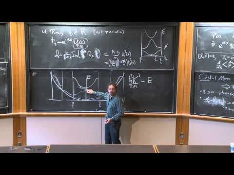
Metals, Insulators, and Semiconductors
This foundational lecture establishes the electronic band theory crucial for understanding the behavior of metals, insulators, and semiconductors, setting the stage for subsequent material science topics.
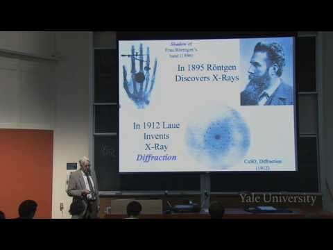

X-Ray Diffraction
Building on electronic properties, this lecture introduces X-ray diffraction, a fundamental technique for experimentally determining the atomic and molecular structure of materials.
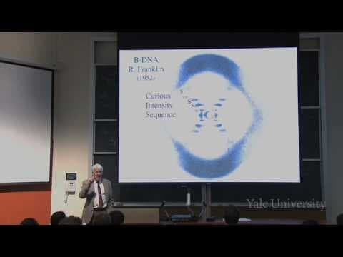
Seeing Bonds by Electron Difference Density
Extending X-ray diffraction, this lecture delves into electron difference density, providing a deeper understanding of chemical bonding and electron distribution within the material structures previously analyzed.
Step 4·Caltech·Carver Mead· 1:33:08

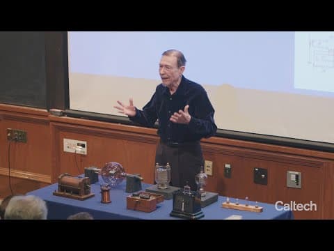
Physics of Computation and Lessons from the Early Days of Semiconductors
With a grasp of material structure and electronic behavior, this lecture explores the historical development and physical limits of semiconductor technology, linking fundamental physics to practical computation.
Step 5·Vanderbilt University·Justus Ndukaife· 50:12
Nanophotonics and Metasurfaces for Advanced Sensing and Imaging
Transitioning from traditional semiconductors, this lecture introduces nanophotonics and metasurfaces, showcasing how advanced material design enables novel optical sensing and imaging applications.

Step 6·Royal Institution·Saiful Islam· 1:00:31

Beyond Lithium-Ion: The Future of Energy Storage Materials
Finally, this lecture applies the principles of advanced materials science to the critical challenge of energy storage, exploring next-generation battery and solar cell technologies beyond current limitations.
Companion reading for this sequence
Amazon Associate
